- 您现在的位置:买卖IC网 > Sheet目录3753 > ATMEGA169P-16MCHR (Atmel)MCU AVR 16KB FLASH 16MHZ 64-VQFN
PIC16F946
DS41265A-page 254
Preliminary
2005 Microchip Technology Inc.
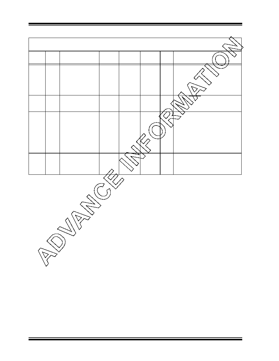
TABLE 19-16: PIC16F946 A/D CONVERSION REQUIREMENTS
Standard Operating Conditions (unless otherwise stated)
Operating Temperature
-40°C
≤ TA ≤ +125°C
Param
No.
Sym
Characteristic
Min
Typ
Max
Units
Conditions
130
TAD
A/D Clock Period(2)
1.6
—
μsTOSC-based, VREF ≥ 3.0V
3.0*
—
μsTOSC-based, VREF full range
130
TAD
A/D Internal RC
Oscillator Period
3.0*
6.0
9.0*
μs
ADCS<1:0> = 11 (RC mode)
At VDD = 2.5V
2.0*
4.0
6.0*
μsAt VDD = 5.0V
131
TCNV
Conversion Time
(not including
Acquisition Time)(1)
—11
—
TAD
Set GO/DONE bit to new data in A/D
Result register
132
TACQ
Acquisition Time
5*
11.5
—
μs
μs The minimum time is the amplifier
settling time. This may be used if the
“new” input voltage has not changed
by more than 1 LSb (i.e., 4.1 mV @
4.096V) from the last sampled
voltage (as stored on CHOLD).
134
TGO
Q4 to A/D Clock
Start
—TOSC/2
—
If the A/D clock source is selected as
RC, a time of TCY is added before
the A/D clock starts. This allows the
SLEEP
instruction to be executed.
*
These parameters are characterized but not tested.
Data in ‘Typ’ column is at 5V, 25
°C unless otherwise stated. These parameters are for design guidance
only and are not tested.
Note 1:
ADRESH and ADRESL registers may be read on the following TCY cycle.
2:
See Table 12-1 for minimum conditions.
发布紧急采购,3分钟左右您将得到回复。
相关PDF资料
2-1546217-0
TERM BLK RCPT 20POS SIDE 5.08MM
1-1546217-9
TERM BLK RCPT 19POS SIDE 5.08MM
1-1546217-8
TERM BLK RCPT 18POS SIDE 5.08MM
1-1546217-7
TERM BLK RCPT 17POS SIDE 5.08MM
1-1546217-6
TERM BLK RCPT 16POS SIDE 5.08MM
1-1546217-5
TERM BLK RCPT 15POS SIDE 5.08MM
1-1546217-4
TERM BLK RCPT 14POS SIDE 5.08MM
1-1546217-3
TERM BLK RCPT 13POS SIDE 5.08MM
相关代理商/技术参数
ATMEGA169P-16MCU
功能描述:8位微控制器 -MCU AVR 16KB, 512B EE 16MHz 1KB SRAM, 5V
RoHS:否 制造商:Silicon Labs 核心:8051 处理器系列:C8051F39x 数据总线宽度:8 bit 最大时钟频率:50 MHz 程序存储器大小:16 KB 数据 RAM 大小:1 KB 片上 ADC:Yes 工作电源电压:1.8 V to 3.6 V 工作温度范围:- 40 C to + 105 C 封装 / 箱体:QFN-20 安装风格:SMD/SMT
ATMEGA169P-16MU
功能描述:8位微控制器 -MCU AVR 16K FLASH 512B EE 1K SRAM LCD ADC RoHS:否 制造商:Silicon Labs 核心:8051 处理器系列:C8051F39x 数据总线宽度:8 bit 最大时钟频率:50 MHz 程序存储器大小:16 KB 数据 RAM 大小:1 KB 片上 ADC:Yes 工作电源电压:1.8 V to 3.6 V 工作温度范围:- 40 C to + 105 C 封装 / 箱体:QFN-20 安装风格:SMD/SMT
ATMEGA169P-16MU SL383
制造商:Atmel Corporation 功能描述:MCU 8BIT ATMEGA RISC 16KB FLASH 3.3V/5V 64PIN MLF - Tape and Reel
ATMEGA169P-16MUR
功能描述:8位微控制器 -MCU AVR LCD 16KB FLSH EE 512B 1KB SRAM-16MHZ RoHS:否 制造商:Silicon Labs 核心:8051 处理器系列:C8051F39x 数据总线宽度:8 bit 最大时钟频率:50 MHz 程序存储器大小:16 KB 数据 RAM 大小:1 KB 片上 ADC:Yes 工作电源电压:1.8 V to 3.6 V 工作温度范围:- 40 C to + 105 C 封装 / 箱体:QFN-20 安装风格:SMD/SMT
ATMEGA169P-8AU
制造商:ATMEL 制造商全称:ATMEL Corporation 功能描述:Microcontroller with 16K Bytes In-System Programmable Flash
ATMEGA169P-8MU
制造商:ATMEL 制造商全称:ATMEL Corporation 功能描述:Microcontroller with 16K Bytes In-System Programmable Flash
ATMEGA169PA
制造商:ATMEL 制造商全称:ATMEL Corporation 功能描述:8-bit Microcontroller with 16K Bytes In-System Programmable Flash
ATMEGA169PA_1
制造商:ATMEL 制造商全称:ATMEL Corporation 功能描述:High Endurance Non-volatile Memory segments